Table of Contents
| Table of Contents |
|---|
Digital Logic Overview
Digital, or boolean logic, logic represents signals in an ideal digital circuit, where the signals can are typically in one of two states or levels [1]. Digital logic allows modern complex problems in electrical circuit designs and programming to be deconstructed into simple binary queries [2].
Digital Logic States (Logic Levels)
In digital circuits, inputs input and outputs output signals can only inhabit a single logic level at any time [3]. These logic levels, or states, are usually represented by the voltage difference.
Binary (Two-Level) Logic
In binary logic, multiple different sets of names are used for the "Highhigh" and "Lowlow" states depending on if the application is in a field of mathematics, computer science, electronics, engineering, etc [4].
Tri-State (Three-State) Logic
In tri-state logic circuits, inputs input and outputs signal output signals can be in a third state along with the binary “High” “high” and “Low” “low” states [5]. This third state is the “High“high-Impedance” impedance” state. An I/O pin/port/pad that is in this state is practically removed from the circuit as if it was were not there in the first place. In this state, a digital signal on the pin/port/pad’s line would not affect the rest of the circuit. This allows multiple circuits’ circuits' I/O pin/port/pads to share lines between them. This is done by having one circuit use the line at a time, while the other circuit’s pin/port/pads on the shared line are in a “High“high-Impedance” impedance” state.
| Digital Logic States | Alternative Names | ||
|---|---|---|---|
| Logical High | Logic '1' | TRUE | ON |
| Logical Low | Logic '0' | FALSE | OFF |
| High Impedance | Hi-Z | Floating | Tri-Stated |
Logic Gate Symbols
Logic gates can have different numbers of inputs, but the summary table will use 2-input logic gates, with the exception of the 1-input Buffer buffer and NOT logic gates. Logic gates can be used in different configurations to create complex digital logic circuits and some logic gates can even be used to create other logic gates.
| XOR Gate Equivalent Circuit Constructed With NAND Gates [6] |
|---|
|

Standards
There have been many different standards for logic gates gate symbols depending on the region and time period it was used in. However, there are 2 two sets of symbols that are currently the most commonly used [7].
| Standard | Symbols | Description | ||
|---|---|---|---|---|
ANSI/IEEE Std 91a-1991 ANSI/IEEE Std 91-1984 MIL-STD-806B |
| This is the traditional and more widely used set of logic gate symbols, where each basic gate (Buffer, OR, AND, XOR) has a distinctive shape. Gates that are the result of combining a NOT gate and one of the basic gates have a circle in front of the distinctive basic gate (NOT, NOR, NAND, XNOR) to represent the complement logic. | ||
IEC 60617-12:1997 ANSI/IEEE Std 91/91a-1991 ANSI Y32.14 |
| These less common standards specify logic gate symbols to be in a rectangular shape with its corresponding function centered inside the rectangle. This design allows for a |


| broader range of devices with more complex functions than with the basic distinctive shape symbols. In this design, inverse logic gates are identified with a line connecting the output signal line upwards to the vertical edge of the rectangle on the same side to create a right-angle triangle. Depending on the standard this “triangle” notation may also be interchangeable with a circle notation similar to the distinctive shape design. |
Truth Tables
A truth table is used to present the all the possible outputs corresponding to any combination of inputs for digital logic problems [1]. Truth tables are usually formated starting with all input values of Logic '0' and increasing the inputs by binary one for each row down the table until all inputs are Logic '1'. They can be used to represent individual gates or complex logic circuits with mutiple gates.
| Half Adder Logic Circuit and Truth Table [9] |
|---|
|

Boolean Algebra
Boolean Algebra algebra can be used to represent and analyze binary (0 and 1) logic circuits [10]. Boolean expressions or equations of logic circuits can be used to calculate the output signals of that circuit, given the input signals without needing to know the exact layout of the circuit.
As boolean algebra is an a different branch of algerbraalgebra, it has its own set of operators, laws, and theorems [3]. These laws and properties create techniques that allow certain boolean expressions of logic circuits to be greatly simplified. As such, different digital logic circuits may have the same simplified boolean equation.
| Half Adder Boolean Equation |
|---|
Boolean Operator Logic Symbols
Similar to logic gates symbols and states, operators operator symbols can greatly vary depending on the region, time period, field of study, and application.
| Basic Alternative Boolean Operator Logic Symbols [11] [12] [13] [14] [15] | |||
|---|---|---|---|
| Negation/Complement (NOT) | Conjunction (AND) | Disonjunction (OR) | Exclusive Disonjunction (XOR) |
Basic Logic Gates Summary Table
Name | Gate Symbol | Truth Table | Description | Example Boolean Equation | ||||||||||||||||||||
|---|---|---|---|---|---|---|---|---|---|---|---|---|---|---|---|---|---|---|---|---|---|---|---|---|
| Buffer Gate |
|
| A 1-input Buffer gate leaves the digital signal unchanged and outputs the same value as the input value. | |||||||||||||||||||||
| NOT Gate |
|
| A 1-input NOT gate, also known as an Inverter, outputs the opposite value of the input. | |||||||||||||||||||||
OR Gate |
|
| A 2-input OR gate outputs a Logic '1' if any input value is Logic '1'. | |||||||||||||||||||||
AND Gate |
|
| A 2-input AND gate outputs a Logic '1' only if both input values are Logic '1'. | |||||||||||||||||||||
NOR (NOT-OR) Gate |
|
| A 2-input NOR gate outputs a Logic '0' if any input value is is Logic '1'. | |||||||||||||||||||||
NAND (NOT-AND) Gate |
|
| A 2-input NAND gate outputs a Logic '0' only if both input values are Logic '1'. | |||||||||||||||||||||
XOR (Exclusive-OR) Gate |
|
| An 2-input XOR gate outputs a Logic '1' only if both input values are the opposite of each other. | |||||||||||||||||||||
| XNOR (Exclusive-NOR) Gate |
|
| An 2-input XNOR gate outputs a Logic '0' only if both input values are the opposite of each other. | |||||||||||||||||||||


Digital Output Configurations
| Output Modes | Diagram | Description | ||
|---|---|---|---|---|
| Push-Pull (Totem-Pole) |
| Push- |
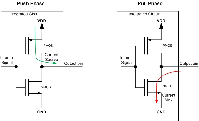
pull is the most common output configuration where an output pin drives a logical " |
high" or " |
low" level [24]. In the |
push phase, the output pin "pushes" the power supply voltage so that the pin sources (supplies) current to the load connected to the output. In effect, this drives the signal on the output line to a " |
high" state. In the |
pull phase, the output pin "pulls" to ground so that the pin sinks (absorbs) current from the load connected to the output. In effect, this drives the signal on the output line to a " |
low" state. | ||||
| Open-Drain |
| In |

an open- |
drain configuration, the output pin is typically connected to the drain terminal of a N-Channel MOSFET. As a result, the output pin can only drive a " |
low" level, but can also assume a " |
high- |
impedance" state [24]. When the drain terminal is closed (connected to ground), the output pin is then pulled to ground so the output pin sinks current from the load. In effect, this drives the output line signal to a " |
low" state. When the drain terminal is open (not connected to ground), the output pin, and therefore the load, is left floating as the line is not connected to the " |
high" or " |
low" level |
voltages. Therefore, it is said the output pin is in a Hi-Z state. | ||||
| Open-Collector |
| In |

| an open- |
| collector configuration, the output pin's functionality is the same as in |
| open- |
| drain. However, in |
| an open- |
| collector configuration, the output pin is typically connected to the collector terminal of a NPN BJT instead of the drain terminal of a NMOS. |
References
[1] J. Braza, “What is Digital Logic?,” Circuit Basics, 28-Jun-2020. [Online]. Available: https://www.circuitbasics.com/what-is-digital-logic/. [Accessed: 01-Apr-2021].
[2] SFUptownMaker, “Digital Logic,” Sparkfun, 03-Oct-2013. [Online]. Available: https://learn.sparkfun.com/tutorials/digital-logic/all. [Accessed: 13-Apr-2021].
[3] T. R. Kuphaldt, Lessons In Electric Circuits, Volume IV – Digital, Fourth., vol. IV, VI vols. 2007.
[4] “Digital Logic Gates,” Electronics Tutorials. [Online]. Available: https://www.electronics-tutorials.ws/logic/logic_1.html. [Accessed: 01-Apr-2021].
[5] Techopedia, “What is Three-State Logic? - Definition from Techopedia,” Techopedia, 07-Jul-2015. [Online]. Available: https://www.techopedia.com/definition/22641/three-state-logic. [Accessed: 13-Apr-2021].
[6] Inductiveload, XNOR from NAND.svg. 2009. Available: https://commons.wikimedia.org/wiki/File:XNOR_from_NAND.svg.
[7] W. McAllister, “Digital logic gates,” Spinning Numbers. [Online]. Available: https://spinningnumbers.org/a/logic-gates.html. [Accessed: 13-Apr-2021].
[8] A. Saleh, “Electronics Done Quick 7 | Logic Gates,” RobotShop Community, 31-Aug-2019. [Online]. Available: https://www.robotshop.com/community/tutorials/show/electronics-done-quick-7-logic-gates. [Accessed: 13-Apr-2021].
[9] E. Coates, “Building a Half Adder,” Raspberry Pi Learning, 23-Jan-2018. [Online]. Available: https://projects.raspberrypi.org/en/projects/halfadder. [Accessed: 13-Apr-2021].
[10] “Boolean Algebra,” Tutorialspoint. [Online]. Available: https://www.tutorialspoint.com/computer_logical_organization/boolean_algebra.htm. [Accessed: 13-Apr-2021].
[11] R. M. Meyer, Introduction to Computer Hardware and Organization . Buffalo, New York, 2002.
[12] “Boolean Algebra (Boolean Expression, Rules and Examples),” BYJUS, 2020. [Online]. Available: https://byjus.com/maths/boolean-algebra/. [Accessed: 13-Apr-2021].
[13] “Comprehensive List of Logic Symbols,” Math Vault, 20-Jul-2020. [Online]. Available: https://mathvault.ca/hub/higher-math/math-symbols/logic-symbols/. [Accessed: 13-Apr-2021].
[14] “Logic Symbols,” RapidTables. [Online]. Available: https://www.rapidtables.com/math/symbols/Logic_Symbols.html. [Accessed: 13-Apr-2021].
[15] H. Yan, “Appendix List of Basic Logic Symbols,” in Spatial similarity relations in multi-scale map spaces, Springer International Publishing, 2015, pp. 187–188.
[16] Stefan506, Logic-gate-buf-us.png. 2005. Available: https://commons.wikimedia.org/wiki/File:Logic-gate-buf-us.png.
[17] Stefan506, Logic-gate-inv-us.png. 2005. Available: https://commons.wikimedia.org/wiki/File:Logic-gate-inv-us.png.
[18] Stefan506, Logic-gate-or-us.png. 2005. Available: https://commons.wikimedia.org/wiki/File:Logic-gate-or-us.png.
[19] Stefan506, Logic-gate-and-us.png. 2005. Available: https://commons.wikimedia.org/wiki/File:Logic-gate-and-us.png.
[20] Stefan506, Logic-gate-nor-us.png. 2005. Available: https://commons.wikimedia.org/wiki/File:Logic-gate-nor-us.png.
[21] Stefan506, Logic-gate-nand-us.png. 2005. Available: https://commons.wikimedia.org/wiki/File:Logic-gate-nand-us.png.
[22] Stefan506, Logic-gate-xor-us.png. 2005. Available: https://commons.wikimedia.org/wiki/File:Logic-gate-xor-us.png.
[23] Stefan506, Logic-gate-xnor-us.png. 2005. Available: https://commons.wikimedia.org/wiki/File:Logic-gate-xnor-us.png.
[24] Y. Stoyanov, “Open Drain Output vs. Push-Pull Output,” Open4Tech, 18-May-2019. [Online]. Available: https://open4tech.com/open-drain-output-vs-push-pull-output/. [Accessed: 13-Apr-2021].
Contributors:
Contributors Summary columns lastupdate order editTime
Faculty Advisors: John Thistle, Kim Pope, Vincent Gaudet, Micheal Lenover (alumni), Allyson Giannikouris